


Material Analysis Service
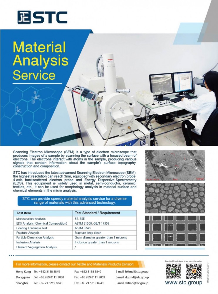
Scanning Electron Microscope (SEM) is a type of electron microscope that produces images of a sample by scanning the surface with a focused beam of electrons. The electrons interact with atoms in the sample, producing various signals that contain information about the sample's surface topography, construction and composition. STC has introduced the latest advanced Scanning Electron Microscope (SEM), the highest resolution can reach 3nm, equipped with secondary electron probe, 4-axis backscattered electron probe and Energy Dispersive-Spectrometry (EDS). This equipment is widely used in metal, semi-conductor, ceramic, textiles, etc., it can be used for morphology analysis in material surface and chemical elements in the micro analysis. STC can provide speedy material analysis service for a diverse range of materials with this advanced technology.


